New!!! Site Search

(These links pertain to my Hobbies!)

BuiltWithNOF
Phasing

Bob Green’s Web Site!

Under Construction

Click picture to enlarge.

Under Construction!

The Above Picture is a typical dipiction of a Dual Path Phase Combined System.

Some manufacturers use only 2 coaxial switches on the input side instead of 3 to reduce system cost, but the general function of the system is the same.

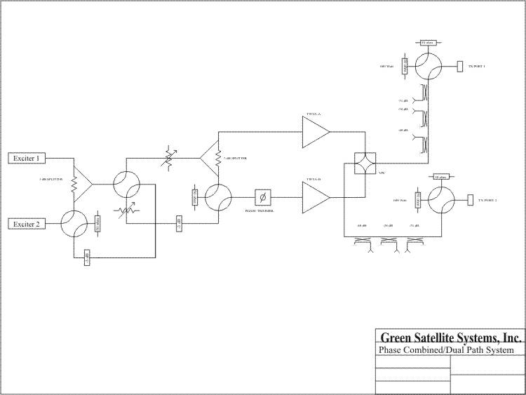
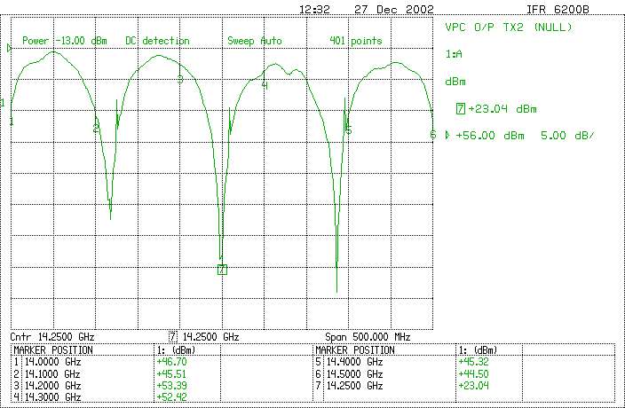
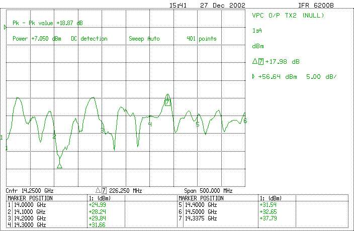
     In the old days of Transportable Satellite Uplinking (1980’s), Phase Combining was considered somewhat of a “Black Art.”  It was necessary because Satellites needed a lot of power to saturate the transponder.  In the ‘90s the satellites got “hotter” and the need for phase combining lessened to the occasional Hurricane/Storm uplink due to rainfade.  With the advent of digital there is an interest in Phase Combining that is twofold. The VPC offers the user flexible “Dual Path” switching and in the phase combined mode offers a “soft fail” feature that eliminates the “switch glitch” encountered with the baseball switch transition in a purely redundant system (more on this later).

     This Tutorial should de-mystify the process and provide you with the understanding necessary to set up and maintain your phase combined system.

(Of course, we offer this service as well.)

     There are two types of Phasing that can be done: 

  1. Narrow Band Phasing
  2. Wide Band Phasing.

     Narrow Band Phasing is the result of transmission line differences in the two HPA paths that requires the need to adjust the Phase shifter almost every time you change frequencies. In other words, the Null Characteristic of the phase combined system is adjusted so only a narrow range of frequencies is aligned in the phasing process.

     Wide Band Phasing is the result of adjusting the transmission lines in the two HPA paths so that the wavelengths are aligned at any frequency in the operational band.  This in turn allows the Null Characteristic to be good no matter what range of frequencies is selected in the operational band. Phase shifter adjustment may not be necessary for long periods of time.  This also provides for the timing involved when modulating intelligence onto a carrier. When all of the Wavelengths in a given band are phased, the modulation between the two transmission lines is also in sync.


This is “NARROW BAND PHASING!”

Click picture to enlarge.

     This is a sample of really bad phasing. Some Systems Engineers,  Integrators and Manufacturers truly believe this is the correct and the only way to phase combine. They are truly mistaken and do not understand what is occurring. Phasing in this manner requires the adjustment of the phase shifter each time you change frequencies and gives no thought whatsoever to the intelligence that is modulated onto the carrier.

   This plot shows multiple null points within a standard 500MHz Ku Bandwidth (14-14.5 GHz).  As the phase shifter is adjusted, these null points move up and down within the spectrum giving the user the illusion that he is “in phase.” This is not the case.  It took an additional 5 feet of semi-rigid cable on the “A” side to correct this problem.  Any “intelligence” that was modulated onto the carrier was “out of sync” within the time domain.

     Note the Reference Line and the dB/division indications.  The reference line is at 56dBm (about 400w).  Normally this line would be at 57 dBm (500w), however, one of the tubes in this system started to saturate at the low end of the band at about 225w, so the output of the higher output HPA was lowered to match the lower o/p unit (also...the system had only been on for about an hour at this point).

     The “null points” are 25, 35 & 37 dB lower than the reference line (400w) which means at those frequencies the “Rejected Power” is about 200mW (marker 7) out of 400W.


This is “WIDE BAND PHASING!”

Click picture to enlarge.

     This is the same system after phasing.  The response “LOOKS” bad but an examination of the data indicates that the “Reject Power” is at least 20dB below our reference line, 56.64 dBm (461W), for most of the band.  Please keep in mind that the two plot examples above are plots of the NULL port...not the TRANSMIT port.  (Note:  our reference line went up 0.64 dB because the system had been on for about 4 hours at this point and the power level of the low o/p HPA had come up some.)  The variations in this plot are not multiple “nulls” as in the first but rather a single null that has been opened up to be wide enough to cover the 14.0-14.5 GHz transmit band.  What you are seeing are system variations in gain and output power as well as the isolation variations within the VPC itself. What this really means is no matter where a signal is applied for amplification within the band, our reject power should be less than 6 watts (marker 7).  This also means that any “intelligence” that has been modulated onto the carrier will be “in sync” within the time domain.

     Ideally we would like to see at least 25 dB of isolation between the output(Transmit) and reject(Null) ports of the Phase Combiner. Unfortunately, we live in a real world where all TWTs are not “New” and cable lengths between the common source and the HPAs are not as short as we would like (less than 5-7 feet is optimum). There are also irregularities in SSA(solid state amplifier) gain variation, Waveguide VSWR variations, VPC Isolation Variations, Etc. About 70% of the bandwidth is at -25dB or better so the few points that are above are just a “fact of life.” For those of you who like to “tweek” the phasing and have the front panel adjustment, small adjustments now would allow you to go from about 6 watts down to a few hundred mW.  However, that 6 watts that you pick up is not likely to make or break your feed!

     Notice that the “delta” marker is about 37 dB below the reference line. The typical Isolation of a Variable Phase Combiner (VPC) is 40 dB between Output and Reject ports, so this would be a typical “maximum” isolation level in any phasing plot you would see.

New Site Search!!!